Aeonix designs printed circuit boards in Kolkata and takes them from schematic to assembled, tested hardware. We lay out boards of up to six layers and more, have the bare boards made by our fabrication partner, and assemble, reflow and bring them up in our own workshop at Boral.
The boards are not a side line. Every one of our 500+ IoT vending machines runs on a board we designed, and so do the surveillance devices we build for the Indian Army. We design for the conditions our own hardware meets in the field, and we bring the same rules to your board.
What we deliver
- Schematic and multilayer layout, up to 6+ layers
- KiCad, Altium Designer, EasyEDA, Fusion 360/Eagle
- Bare boards from our fabrication partner
- Assembly and reflow in our Boral workshop
- Bring-up, testing and firmware
- Prototypes in 3–4 weeks
What we design
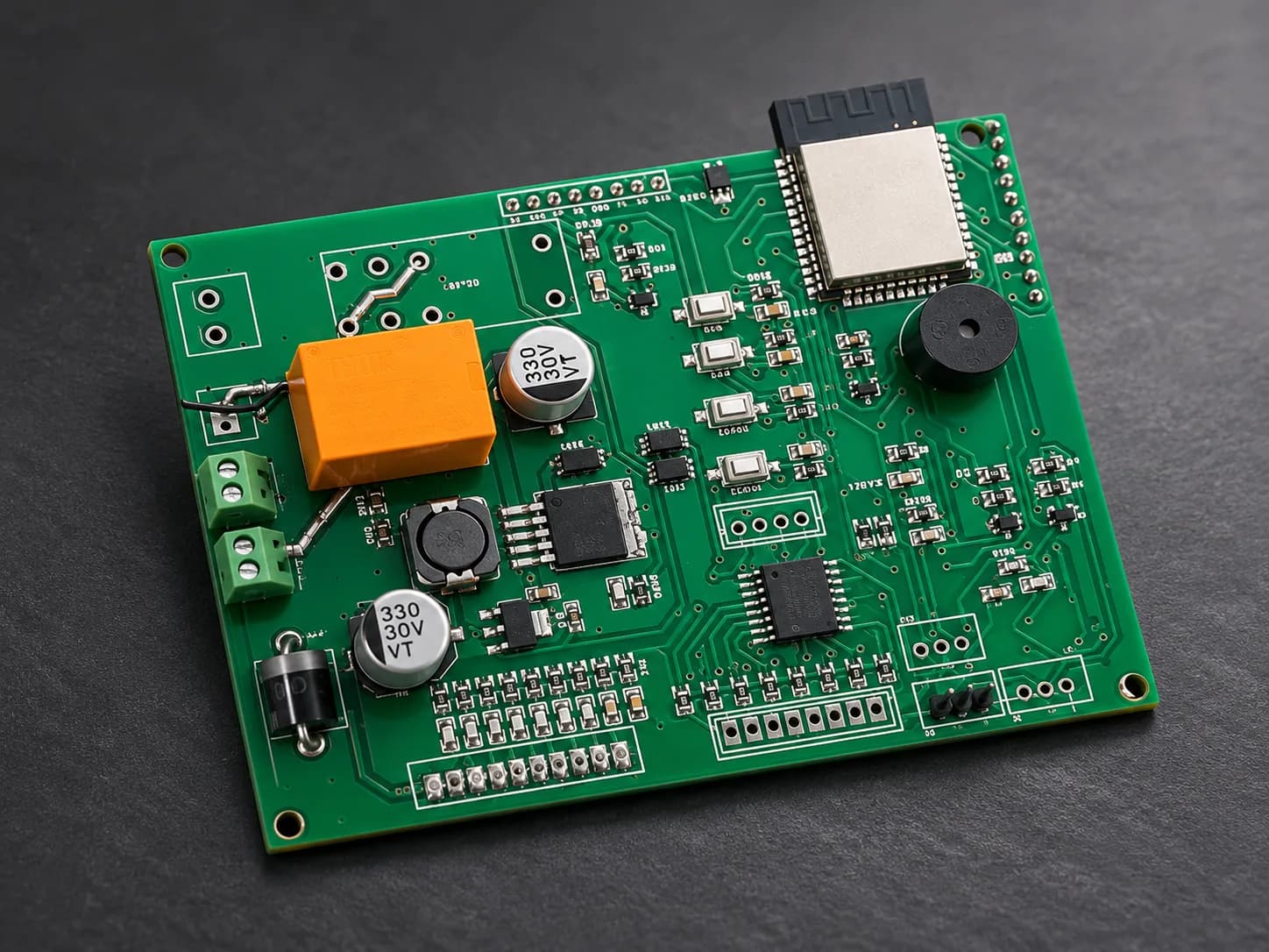
Five of our board designs are in production today: ESP32-based controllers, Quectel 4G LTE communication modules, motor drivers with battery management, and custom display drivers. We design multilayer boards of up to six layers and more, from the schematic and component choice through layout to the files your manufacturer needs. Where a standard module is the right choice, such as a cellular modem, we design the board around it.
- Schematic capture and component selection
- Multilayer layout, up to 6+ layers
- Boards built around Wi-Fi, BLE, GSM, 4G LTE and LoRa modules
- Motor-drive and battery-management boards
- Manufacturing files: Gerbers, drill files, BOM and pick-and-place
Tools we work in
We design in KiCad, Altium Designer, EasyEDA and Fusion 360 (Eagle). We can start a board from scratch in whichever tool suits the project, or pick up an existing design in the format your team already uses.
Fabrication, assembly and testing
Bare boards are made by our fabrication partner. Assembly and reflow happen in our workshop at Boral, Kolkata, which also has bench supplies, oscilloscopes and 3D printing. The engineers who designed a board bring it up, write its firmware, and are the ones who debug it if it ever fails in the field.
- Bare boards from our fabrication partner
- Assembly and reflow in our Boral workshop
- Bring-up and testing on the bench
- Firmware in C/C++, on an RTOS or bare metal, with over-the-air updates
Designed for Indian power and weather
Our design rules come from our own field failures, not datasheets. We have measured mains swinging between 178 V and 268 V on one line within an hour, so our boards use wide-input power supplies (90–305 V), at least 4 kV of surge protection and a raised brownout threshold. Boards that go outdoors are conformally coated and sealed in IP65 housings.
Turnaround and quantities
A prototype typically takes three to four weeks. A minimum order quantity applies, and we confirm it in the quote together with the build and test plan. You can bring us in for the board alone, or for the board with its firmware, enclosure and cloud as one project.
Our boards in the field, across India
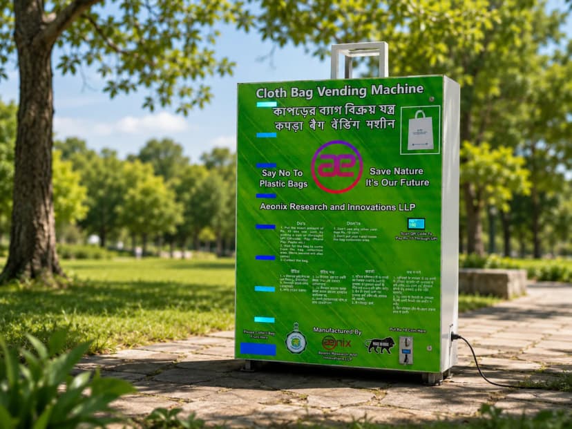
- 500+ IoT vending machines for the West Bengal, Sikkim and Central Pollution Control Boards run on our boards
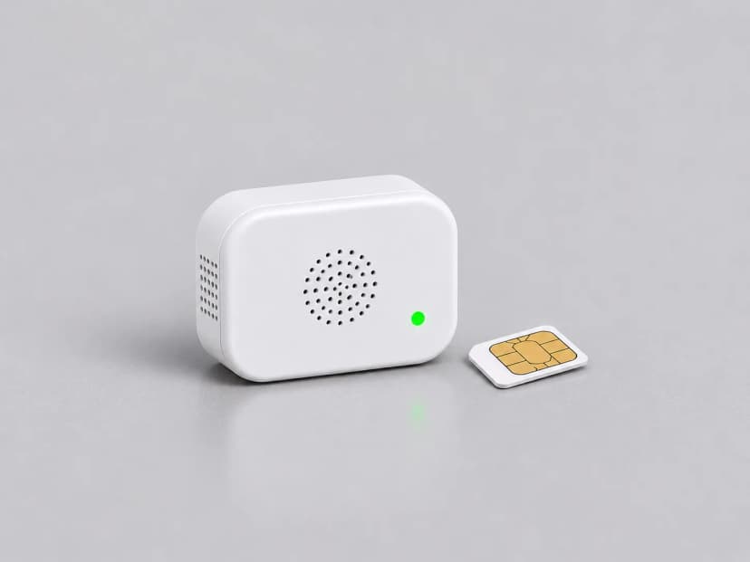
- 4G surveillance and audio-monitoring devices for the Indian Army and security agencies are built around our PCBs
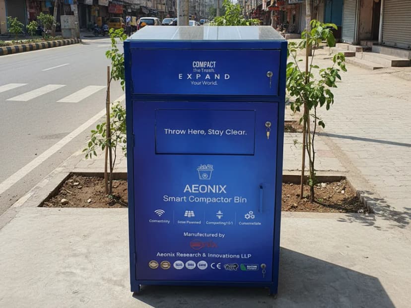
- Our solar compactor bins use a multilayer, conformally coated board in an IP65 enclosure